Due to changes over time and variation across industries and education the nomenclature used to describe this format does vary and bare die are also known as:
- Unencapsulated die
- Unencapsulated chip
- Bare chip
- Chip level
- Die level.
Unlike packaged semiconductors which form >99% of active component usage, working with the bare die form involves additional complexity across multiple disciplines:
- Electrical engineering
- Mechanical engineering
- Quality Management
- Component Selection
- Commercial.
However, there are significant potential benefits working at bare die level if these complexities are understood and are well managed.
Benefits of bare die
The benefits of bare die can be broadly summarized as:
- Size reduction &/or increased integration
- Potential for improved power management
- Potential for improved electrical performance
- Potential for operation at temperature extremes
- Can be assembled to achieve high mechanical ruggedness / reliability.
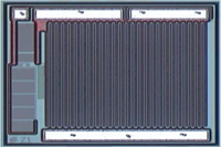
Bare die typically end up in five main usages:
- SiP - System-in-Package
- MCM - Multiple-Chip-Module (Plastic)
- MCM - Multiple-Chip-Module (Ceramic)
- Hybrid Circuit - Thick Film & LTCC
- COB / COG / COF - Chip-On-Board, Chip-On-Glass, Chip-On-Flex
Each usage is driven by a slightly different combination of benefits, please review the above links for more information on each use.
Challenges of bare die
1) One of the most commonly made mistakes is the assumption that if a package part exists then the bare die inside that package is automatically available. Whilst it may be true that wafers are being produced in order to assemble that packaged part it does not mean that that semiconductor maker has the technical means, commercial desire or will be willing to warrant and fund the support in the bare die format. You can use our parametric tool to find parts with availability.
2) The second most commonly made mistake is that the bare die will by default be lower cost than the finished package.
However this is not the case for three principle reasons:
- Volume manufacturing flows that make packages cannot be easily automated to test and release bare die
- Non-standard product must undertake a specialized flow both for engineering and quality before release
- Manufactures prevent 3rd parties using lower cost bare die to assemble themselves into competing packages and erode the market price.
It's usually only at very high annual production volume that bare die are priced either on par or lower than the packaged part.
In many instances it also means that the minimum order quantities required to release a part in the bare die form may be higher than anticipated, this is due to the economic trade-offs and business model of each individual semiconductor maker.
This means that due care should be taken in terms of selecting and building first bills of material. Our selector guide includes an MOQ indicator which can help assist with finding the right parts.
3) The commercial market and accompanying volumes ultimately drive wafer production and the creation and maintenance of part numbers. This means that obsolescence is often a direct function of reduced commercial demand and is irrespective of your application or industry sector. This can impact non-commercial market applications and those with low volumes. Please see our section for long term bare die support of existing applications.
4) Bare die are always produced to suit the manufacturers volume assembly process with little to no chance of customization. This may mean in some instances that there is limited or no test coverage at the wafer level due to there being 100 % test in the packaged format. It may also mean that the die needs mechanical modification or sensitive handling, such as adding bumps for flip-chip or additional wirebonding consideration due to metal alloy or sensitive active underlying pad areas. Diedevices can help in terms of wafer testing and also provide solutions for bumping or other mechanical modifications to suit your intended assembly process.