The principal technical drivers for choice of bare die format:
- Mechanical design requirements
- Ability to modify the die to suit the application
- Level of test or point of test
- Compatibility with the chosen assembly process and associated build
Non-technical aspects such as commercial bare die availability are covered elsewhere in the site.
Mechanical design requirements
Whilst the vast majority of bare die in the semiconductor industry end up assembled in a package, a much smaller percentage are released to purchase alongside the package in their un-encapsulated form. All bare die supported in the market are mechanically defined by their primary use, which for the vast majority is assembly into the commercial package. The general rule is that a bare die's mechanical specification is a direct function of the die-to-package interconnect method and interconnect materials used to assemble the commercial package. There are some applications where die are released specifically for un-encapsulated assembly however these are the exceptions. Additionally, unless there are high volumes involved it's not usually possible to have the die producer customize the mechanical specification from it's primary release.
Below gives guidance as to the typical bare die mechanical specifications determined by industry standard package assembly methods:
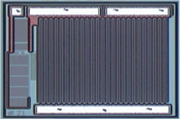
Wirebonded packages
Die use bonding pads of a thickness and metal stack mix that's compatible with most industry standard wire-bonding processes and wire materials. This provides versatility in terms of production method and scope to use different wire-bonding techniques, pitches and wire sizes where the design requires it. Historically bond pads are majority Al or Au with equivalent bonding process and wire material choices. Mature products will almost certainly continue to be produced this way.
However, this is evolving for newer wire-bonding die designs with some assembly processes now running assembly with Cu bond-wires and the die design building the bondpad stacks with matching Cu. Using a bare die metalized with Cu bond pads means additional consideration must be given to wirebond profile due extra hardness of the bondpads. Cu bondpads are also much more susceptible to oxidisation so additional care needs to be taken at point of bond and to limit bare die exposure to any humidity.
Laminate assembly packages
Bonding pads are raised slightly above the surface of the die and are not primarily intended for wire-bonding. These bonding pads can usually be traditionally wire-bonded but significantly lower forces must be used under high precision control. This is because often in these cases die designers have not allowed for the impact forces of traditional wire-bonding and there may well be sensitive active circuitry directly under the bond pad stack. Conversely there are also cases where a die is dual purposed by design so it can be assembled conventionally or in a laminate variant with no process change.
Flip-chip assembled packages
Bonding pads are either replaced entirely by interconnect bumps or exist as part of a base die design which is configured by the final fabrication layers in the bare die's production process to add interconnect bumps. This may allow production of wire-bondable variants although the more common reason is to give flexibility to product different I/O interconnect routings or enable different functional specification on the active surface of the die. It's usually the case that if a bare die is produced for only flip-chip assembled packages then there will be no wirebondable variant produced or likely to be produced without significant economic investment.
3D integrated packages
The bare die is specifically designed to offer interconnect vertically in one or both directions to other die or interposers. Techniques such as TSV (through-silicon via), routing interposer and vertical wire rails are built as part of the fabrication process to maximise integration at lowest size. These bare die are usually made bespoke for a specific application. However with increased integration demands and applications such as IoT and MEMs mixing more technologies into the same package, it may be expected to see bare die designed with 3D enabled properties which can be used in multiple applications or multiple configurations.
Application specific modification
Thickness
The most common modification made irrespective of the interconnect technique used by the die. All ICs and Discretes essentially use a semiconductor material as base substrate with the active area built upon that. Typically the active die area is a very small percentage of the total thickness, for example a typical Si fabrication may use wafers with thicknesses of 750µm where active area may be only 10s of microns at most. During wafer fabrication thickness is preferred as it provides stability and ease of handling/production.
After fabrication additional wafer thinning is a common process to remove unnecessary excess semiconductor material from the die.
This is done for either:
- Height reduction - Due to package size restrictions, particularly for stacked die
- Improved wafer yields / throughput - Thinner wafers are typically easier process which improves yield and speed
- Flexibility - Extremely thin de-stressed die can accept a degree of warpage required for some die-on-flex applications
- Performance improvement - Such as reducing overall capacitance or improving thermal transfer.
Wafer thinning can reduce a bare die down to single micron digit thicknesses where needed although the process handling at both thinning and post-processing stage increases in complexity. Routinely wafers can be thinned to 250 microns with minimal changes to handling or post-process assembly flow. Below that then managing wafer stress and further die handling start to need to be considered.
To receive bare die with a specific thickness contact us at sales@diedevices.com
Metalization
There are two areas where metalisation may need to be added/modified:
- Bonding pad interface - To enable mono-metalic bonding to reduce risk of intermetallic growth.
- Backside contact of the die - To aid thermal management or to improve conductivity where the die backface as an electrical potential.
- To enable a specific die attach assembly process. E.g. Ti/Ni/Ag alloy for solder attach.
Interconnect method
Bare die interconnect method can be changed by:
- Adding bumps to bare die with wire bonding pads - This converts a wire-bondable die to a flip-chip interconnect die - Done at wafer level as a post fab process. Used to reduce X-Y footprint and to enable multiple die integrations for MCM or SiP.
- Adding an i/o re-distribution layer or interposer - Done at wafer level post-fab as a 3rd party process, can be designed to suit flip-chip, wirebonding or both
- A bumped die cannot easily be converted to wire bondable.
There are several different methods of modifying interconnect the right choice will depend on the application, economics and forward profile. Contact us at sales@diedevices.com for assistance.
Level of test or point of test
Most wafer products historically were tested prior to mechanical modifications such as backside thinning. However this flow can change when the modifications alter interconnect or are intended to deliver a different electrical outcome. It may be that test or re-test needs to occur after mechanical modification and this should be factored into design and yield expectations.
Also depending on the product and reliability level required additional sacrificial layers may be added at the wafer level to enable the device to undergo a fully connected dynamic burn-in or to allow testing on dedicated test pads which are non-essential to the main interconnect of the device.
Compatibility with the chosen assembly process and associated build
All bare die designs need to be viable in terms of yield aspirations, assembly costs and throughput rates. As integration levels increase, also increases the likelihood/requirement to combine a variety of interconnect methods e.g. Wirebonding, Via and flip-chip. Also when die technologies are mixed, the mechanical make up of those die themselves may dictate a particular interconnect method which in turn influences the scope of design. As much as an assembly process needs to be able to realize the design also the design needs to be compatible with the available assembly process.
In summary
Die candidate technical selection can be broadly described by three steps:
- Is the standard mechanical factory output compatible with the design and assembly process?
- Can the standard output be customized where needed to suit the application and assembly process?
- Are there other component /circuit alternatives that present a better solution?