- Wide output swing & high signal-to-noise ratio
- Narrow IDSS range for ease of tolerance in low voltage applications
- 40V breakdown for max linear headroom in high transient program content amplifiers
- Low input noise to capacitance product with nearly zero popcorn noise
Applications:
- Audio amplifiers & pre-amplifiers
- Discrete low-noise operational amplifiers
- Battery operated audio pre-amplifiers
- Guitar pickups, effects pedals, microcphones, audio mixer consoles
- Acoustic sensors & Sonic imaging
- Sonobuoys, hydrophones
- Chemical & radiation detectors
- Instrumentation amplifiers
- Accelerometers
- CT scanner input stage
- Oscilloscope input stage
- Electrometers
- Vibration detectors
Test conditions:
- BVGSS -40V @ IG = -1 mA, VDS = 0V
- IGSS(MAX) -200 pA @ VGS = -30V, VDS = 0V
- |VGS1-VGS2|(MAX) 20mV @ VDS = 10V, ID = 1mA
- VP(MIN) -0.15V @ VDS = 10V, ID = 100 nA
- VP(MAX) -2V @ VDS = 10V, ID = 100 nA
- IDSS(MIN) 2mA @ VDS = 10V, VGS = 0V
- IDSS(MAX) 6.5mA @ VDS = 10V, VGS = 0V
- Gfs(MIN) 8000µS @ VDG = 10V, VGS = 0V, f = 1kHz
- en(MAX) 2.5nV/√Hz @ VDS = 10V, ID = 2000µA, f = 1kHz, NBW = 1Hz
- CISS(MAX) 25pF @ VDS = 10V, ID = µA, VGS = 0V, f = 1MHz
- CRSS(MAX) 5.5pF @ VDS = 10V, VGS = 0V, ID = 0µA, f = 1MHz
Linear Systems
Electrical Datasheet
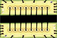
Die Physical Data:
Footprint: 1.137mm² (1763mil²)
Request Pad Layout
- Type: Ultra-low Noise
IGSS: -200pA
|VGS1-VGS2|: 20mV
∆|VGS1-VGS2|/∆T: n/a
VGS(OFF) MIN: -0.15V
VGS(OFF) MAX: -2.0V
IDSS(MIN): 2.00mA
IDSS(MAX): 6.5mA
gfs(MIN): 8,000µS
en: 2.5nV√Hz
CISS(MAX): 25pF
CRSS(MAX): 5.5pF
- Green:Available from stock or at low factory MOQ.
- Amber: Available on factory order with MOQ.
- Red: High factory MOQ may apply, please ask for details.
- Green: This bare die is specified and tested for use in high reliability applications.
- Amber: This bare die can meet higher reliability specifications with additional testing & qualification, please ask for details.
- Red: This bare die is not specified or specifically designed for use in high reliability applications.
- Green: This bare die is qualified for space applications or has space level qualification data, please ask for details.
- Amber: This bare die can be specified for space applications with additional testing and qualification, please ask for details.
- Red: Suitability of this bare die for space applications is unknown and requires further qualification, please ask for details.


