- ** PRODUCT DISCONTINUED **
- Military Temperature Range, -55°C to +125°C for High Reliability
- Break-before-make switch function eliminates channel overlap
- Analog voltage range (VDD - VEE) : 3V to 18V
- ON resistance: 125Ω (typ) over 15VP-P signal
- Matched Switch Characteristics: RON = 10Ω (max), VDD - VEE = 15V
- Binary address decoding on-chip
- Quiescent current : 0.2 µA, VDD = 15V
SiS OBSOLETE
Electrical Datasheet
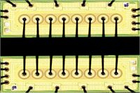
Die Physical Data:
Footprint: 4.651mm² (7208.881mil²)
Request Pad Layout
- Channels: 3
- Bits: 2
- Config: 1:2
- Schmitt Trigger: No
VCC (Max): 18.00V
BW (Max): 30MHz
RON: 125Ω
RON (Max): 240Ω
ICC (Max) @ VNOM: 0.0002mA
- Config: 1:2
- Input Level: CMOS
- Output Level: CMOS
- Channels: 3
- Bits: 2
VCC (Max): 18.00V
RON: 125Ω
BW (Max): 30MHz
ICC (Max) @ VNOM: 0.0002mA
VNOM (Max): 15.0V
- Green:Available from stock or at low factory MOQ.
- Amber: Available on factory order with MOQ.
- Red: High factory MOQ may apply, please ask for details.
- Green: This bare die is specified and tested for use in high reliability applications.
- Amber: This bare die can meet higher reliability specifications with additional testing & qualification, please ask for details.
- Red: This bare die is not specified or specifically designed for use in high reliability applications.
- Green: This bare die is qualified for space applications or has space level qualification data, please ask for details.
- Amber: This bare die can be specified for space applications with additional testing and qualification, please ask for details.
- Red: Suitability of this bare die for space applications is unknown and requires further qualification, please ask for details.


