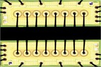
- ** PRODUCT DISCONTINUED **
- Output Drive Capability: 10 LSTTL Loads
- Outputs Directly Interface to CMOS, NMOS, and TTL
- Low Input Current: 1µA
- Operating Voltage Range: 2.0 to 6.0V
- Direct drop-in replacement for obsolete components in long term programs
- FM and FSK modulation & demodulation
- Frequency synthesis and multiplication
- Frequency discrimination
- Tone decoding
- Data synchronization and conditioning
- Voltage–to–frequency conversion
- Motor speed control
Applications:
SiS OBSOLETE
Electrical Datasheet
Die Physical Data:
Footprint: 3.51mm² (5440.511mil²)
Request Pad Layout
- Input Level: CMOS
- Output Level: CMOS
- Bits: 1
VCC (Max): 6.00V
fMIN @ VNOM: 70MHz
tpd (Max) @ VNOM: 37ns
ICC (Max) @ VNOM: 0.04mA
Output Drive (Max): 5.2mA
VNOM (Max): 6V
- Green:Available from stock or at low factory MOQ.
- Amber: Available on factory order with MOQ.
- Red: High factory MOQ may apply, please ask for details.
- Green: This bare die is specified and tested for use in high reliability applications.
- Amber: This bare die can meet higher reliability specifications with additional testing & qualification, please ask for details.
- Red: This bare die is not specified or specifically designed for use in high reliability applications.
- Green: This bare die is qualified for space applications or has space level qualification data, please ask for details.
- Amber: This bare die can be specified for space applications with additional testing and qualification, please ask for details.
- Red: Suitability of this bare die for space applications is unknown and requires further qualification, please ask for details.


