- ** PRODUCT DISCONTINUED **
- Swing Independent of Fanout
- Logic Edge–Clocked Flip–Flop Design — Logic state is retained indefinitely with clock level either high or low; information is transferred to the output only on the positive–going edge of the clock pulse
- Output drive: x2 Low–power TTL Loads or x1 Low–power Schottky TTL Load
- High Input Voltage up to 20V
- Symmetrical Output Characteristics
- Specified at 5V, 10V & 15V
- Suits low power dissipation and/or high noise immunity applications
- Buffered Inputs for high gain & improved transfer characteristics
- ESD protection diodes on Inputs
- Military Temperature Range for High Reliability
SiS OBSOLETE
Electrical Datasheet
Die Physical Data:
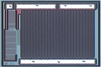
Footprint: 1.930mm² (2990.886mil²)
Request Pad Layout
- Input Level: CMOS
- Output Level: CMOS
- Bits: 2
VCC (Max): 6.00V
fMIN @ VNOM: 8MHz
tpd (Max) @ VNOM: 100.0ns
ICC (Max) @ VNOM: 0.004mA
VNOM (Max): 15.0V
Output Drive (Max): 2.0mA
- Green:Available from stock or at low factory MOQ.
- Amber: Available on factory order with MOQ.
- Red: High factory MOQ may apply, please ask for details.
- Green: This bare die is specified and tested for use in high reliability applications.
- Amber: This bare die can meet higher reliability specifications with additional testing & qualification, please ask for details.
- Red: This bare die is not specified or specifically designed for use in high reliability applications.
- Green: This bare die is qualified for space applications or has space level qualification data, please ask for details.
- Amber: This bare die can be specified for space applications with additional testing and qualification, please ask for details.
- Red: Suitability of this bare die for space applications is unknown and requires further qualification, please ask for details.


