- ** PRODUCT DISCONTINUED **
- Wide supply voltage range 2V-18V
- Maximum supply current 200µA
- No supply current spike during output transition
- Option to reduce external component count versus legacy bipolar 555
- Timing from microseconds through hours
- Accepts higher impedance timing elements than legacy 555 for longer RC time constants
- Operates in both astable and monostable modes
- Adjustable duty cycle
- Output drives TTL/CMOS/MOS
SiS OBSOLETE
Electrical Datasheet
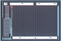
Die Physical Data:
Footprint: 1.560mm² (2418.008mil²)
Request Pad Layout
MIL-STD Qualification:
38534 Class K LAT

- N/A
VS (Min): 2.00V
VS (Max): 18.00V
IQ: 200µA
- Green:Available from stock or at low factory MOQ.
- Amber: Available on factory order with MOQ.
- Red: High factory MOQ may apply, please ask for details.
- Green: This bare die is specified and tested for use in high reliability applications.
- Amber: This bare die can meet higher reliability specifications with additional testing & qualification, please ask for details.
- Red: This bare die is not specified or specifically designed for use in high reliability applications.
- Green: This bare die is qualified for space applications or has space level qualification data, please ask for details.
- Amber: This bare die can be specified for space applications with additional testing and qualification, please ask for details.
- Red: Suitability of this bare die for space applications is unknown and requires further qualification, please ask for details.


