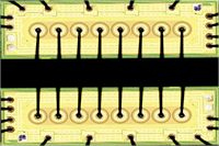
Die Devices is pleased to announce our partnership with Innoscience for support of GaN-On-Silicon Power Transistor bare die products. Innoscience is the world's largest 8-inch wafer manufacturer 100% focused on GaN technology and fully owns and controls the world's largest dedicated 8-inch GaN-on-Si wafer fab. Innoscience's bare die products are fabricated to provide best-in-class performance at lowest cost to customer and benefit from an undiluted engineering focus and technical resources 100% committed to GaN-On-Silicon technology.
Unlike other larger semiconductor vendors, where volume needs of the package discrete business are prioritised over support of the product in bare die form, Innoscience treat the GaN bare die format equally in importance as the packaged discrete. Access to product is flexible with factory MOQs which suit the project need. Conversely when volumes ramp, economies of scale, usage of leading processes and fab production still ensure that product is competitively priced. As there is no link between package part sales and bare die sales volume, the risk of commercial obsolescence impacting wafer availability is lower and only genuine technology obsolescence means a part can't physically be supported.
Product summary available in bare die:
| High Voltage >=650V | Versus Silicon |
|
|
|
|
|
|
| Low Voltage 30V-150V | Versus Silicon |
|
|
|
|
|
|
|
Please use our Parametric Search Tool or select a part from the product family list.

Summary technical benefits:
- Higher performance versus equivalent Silicon MOSFETs
- Smaller die sizes for increased power density in a given area
- Superior thermal performance due to wide bandgap structure.
Summary commercial benefits:
- Low Minimum Order Quantity for prototyping
- Ease of availability for die drawings and support
- Low obsolescence and volume leveraged fab process for lowest cost.