Miltary grade bare die operating -55° to +125° range and is a direct replacement for Texas Instruments TL072M and is a higher reliability replacement for TL072A, TL072/2 and TL072.
Features:
- Low Noise en = 15nV/vHz (typ)
- Low Harmonic Distortion : 0.003% (typ)
- Wide Common-Mode (to VCC+) and Differential Voltage ranges
- Low Input Bias Current and Offset Currents
- High Slew Rate: 16V/µs(typ)
- Internal Frequency Compensation
- High Input Impedance JFET-Input Stage
- Short-Circuit Protection
- Latch-Up Free Operation
- Low power consumption
- Military temperature range
Vendor:
Silicon Supplies
Electrical Datasheet
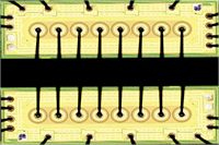
Die Physical Data:
Footprint: 2.296mm² (3558.811mil²)
Request Pad Layout
Silicon Supplies
Electrical Datasheet
Die Physical Data:
Footprint: 2.296mm² (3558.811mil²)
Request Pad Layout
Product Families: Used for this device are tabulated below.
Functional:
- Channels: 2
- Shutdown: No
Specification:
Rail - Rail: VS (Min): 5.00V
VS (Max): 36.00V
Gain BW: 3.00MHz
Slew Rate: 16.0V/µs
VN: 15.0nV√Hz
VOS (Max): 6.000mV
VOS Drift: 18.00µV/°C
IIB (Max): 200.00000nA
IQ per Channel: 1.400mA
IO: 10.0mA
CMRR (Typ): 86dB
VS (Max): 36.00V
Gain BW: 3.00MHz
Slew Rate: 16.0V/µs
VN: 15.0nV√Hz
VOS (Max): 6.000mV
VOS Drift: 18.00µV/°C
IIB (Max): 200.00000nA
IQ per Channel: 1.400mA
IO: 10.0mA
CMRR (Typ): 86dB
Other Detail: Important information for this device is tabulated below.
Traffic light setting for Minimum Order Quantity indicates the following:
- Green:Available from stock or at low factory MOQ.
- Amber: Available on factory order with MOQ.
- Red: High factory MOQ may apply, please ask for details.
Traffic light setting for High Reliability indicates the following:
- Green: This bare die is specified and tested for use in high reliability applications.
- Amber: This bare die can meet higher reliability specifications with additional testing & qualification, please ask for details.
- Red: This bare die is not specified or specifically designed for use in high reliability applications.
Traffic light setting for Space Grade indicates the following:
- Green: This bare die is qualified for space applications or has space level qualification data, please ask for details.
- Amber: This bare die can be specified for space applications with additional testing and qualification, please ask for details.
- Red: Suitability of this bare die for space applications is unknown and requires further qualification, please ask for details.