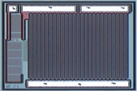
- Ultra-low noise en 1.9nV/√Hz(TYP)
- Low input capacitance CISS 8pF(TYP)
- Low gate leakage, IGSS & IG
- Tight differential voltage match versus current
- Improved operational amplifier speed settling time accuracy
- Minimum input error trimming error voltage
- Lower intermodular distortion
Applications:
- Wideband differential amplifiers
- High-speed temperature compensated single-ended input amplifiers
- High speed comparators
- Impedance converters
Test conditions:
- BVGSS 50V @ IG = 1µA, VDS = 0V
- IGSS(MAX) 100 pA @ VGS = 0V, VDS = -15V
- |VGS1-VGS2|(MAX) 20mV @ VDS = -15V, IG = -1mA
- VP(MIN) 1.5V @ VDS = -15V, ID = -1 nA
- VP(MAX) -3.5V @ VDS = -15V, ID = -1 nA
- IDSS(MIN) 2.5mA @ VDS = -15V, VGS = 0V
- IDSS(MAX) 15mA @ VDS = -15V, VGS = 0V
- Gfs(MIN) 1500µS @ VDS = -15V, VGS = 0V, f = 1kHz
- en(TYP) 1.9nV/√Hz @ VDS = -15V, ID = -2mA, f = 1kHz, NBW = 1Hz
- CISS(TYP) 8pF @ VDS = -15V, ID = -200µA, VGS = 0V, f = 1MHz
- CRSS(TYP) 3pF @ VDS = -15V, VGS = 0V, ID = -200µA, f = 1MHz
Linear Systems
Electrical Datasheet
Die Physical Data:
Footprint: 0.640mm² (992mil²)
Request Pad Layout
- N/A
IGSS: 100pA
|VGS1-VGS2|: 20mV
∆|VGS1-VGS2|/∆T: n/a
VGS(OFF) MIN: 1.5V
VGS(OFF) MAX: 5.0V
IDSS(MIN): -2.5mA
IDSS(MAX): -30mA
gfs(MIN): 1,500mS
en: 1.9nV√Hz
CISS(MAX): 8pF
CRSS(MAX): 3pF
- Green:Available from stock or at low factory MOQ.
- Amber: Available on factory order with MOQ.
- Red: High factory MOQ may apply, please ask for details.
- Green: This bare die is specified and tested for use in high reliability applications.
- Amber: This bare die can meet higher reliability specifications with additional testing & qualification, please ask for details.
- Red: This bare die is not specified or specifically designed for use in high reliability applications.
- Green: This bare die is qualified for space applications or has space level qualification data, please ask for details.
- Amber: This bare die can be specified for space applications with additional testing and qualification, please ask for details.
- Red: Suitability of this bare die for space applications is unknown and requires further qualification, please ask for details.


