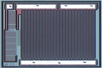
This bare die is an electrical and mechanical replacement for the legacy ON Semi / Motorola (ON, MOT) or Microsemi PPC (MSC, PPC) 2N3715 or 2C3715.
Features:
- Collector current up to 10A
- Gain ranges specified at 1A and 3A
- Low VCE(sat) : 0.5V (typ) at IC = 5A, IB = 0.5A
- Solderable back metal
Applications:
- General purpose power amplification
- Switching of large currents
Vendor:
Silicon Supplies
Electrical Datasheet
Die Physical Data:
Footprint: 6.25mm² (9687.530mil²)
Request Pad Layout
Silicon Supplies
Electrical Datasheet
Die Physical Data:
Footprint: 6.25mm² (9687.530mil²)
Request Pad Layout
Product Families: Used for this device are tabulated below.
Functional:
- N/A
Specification:
V(BR)CEO, VCES: 60.0V
IC(Max): 10.000A
hFE1(Min): 50
hFE1(Max): 150
hFE1 @ IC: 1,000mA
hFE2(Min): 30
hFE2 @ IC: 3,000.00mA
VCE(sat)1(Max): 0.800V
VCE(sat)1 IC/IB: 5/500A/mA
VCE(sat)2(Max): n/a
VCE(sat)2 IC/IB: -A/mA
fT(Min): 4MHz
IC(Max): 10.000A
hFE1(Min): 50
hFE1(Max): 150
hFE1 @ IC: 1,000mA
hFE2(Min): 30
hFE2 @ IC: 3,000.00mA
VCE(sat)1(Max): 0.800V
VCE(sat)1 IC/IB: 5/500A/mA
VCE(sat)2(Max): n/a
VCE(sat)2 IC/IB: -A/mA
fT(Min): 4MHz
Other Detail: Important information for this device is tabulated below.
Traffic light setting for Minimum Order Quantity indicates the following:
- Green:Available from stock or at low factory MOQ.
- Amber: Available on factory order with MOQ.
- Red: High factory MOQ may apply, please ask for details.
Traffic light setting for High Reliability indicates the following:
- Green: This bare die is specified and tested for use in high reliability applications.
- Amber: This bare die can meet higher reliability specifications with additional testing & qualification, please ask for details.
- Red: This bare die is not specified or specifically designed for use in high reliability applications.
Traffic light setting for Space Grade indicates the following:
- Green: This bare die is qualified for space applications or has space level qualification data, please ask for details.
- Amber: This bare die can be specified for space applications with additional testing and qualification, please ask for details.
- Red: Suitability of this bare die for space applications is unknown and requires further qualification, please ask for details.