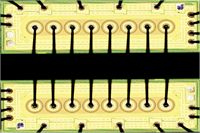
- Ideal for small form factor high integration applications
- Wide supply voltage: VCC 1.65V - 5.5V
- Very low rON : 6Ω Typ, VCC = 4.5V
- High speed: tpd 0.8ns Max, VCC = 3.3V
- Switch current capability: 32mA
- TTL input compatibility (VCC = 3.3V)
- Enable inputs accept up to 5.5V
- Rail-to-Rail Input / Output
- High noise immunity
- Tiny Die size
- Committed long term support with no die mask changes
Applications:
- Analog-to-digital or Digital-to-analog conversion
- Signal gating
- Chopping
- Modulation / De-modulation
Silicon Supplies
Electrical Datasheet
Die Physical Data:
Footprint: 0.389mm² (602.642mil²)
Request Pad Layout
- Channels: 2
- Config: 1:1 SPST
VCC (Max): 5.50V
RON: 6.00Ω
RON (Max): 10.0Ω
BW (Max): 150MHz
VIO (Min): 0.00V
VIO (Max): 5.50V
IIO (Cont): 50mA
ICC (Max) @ VNOM: 10.00µA
- Switch Type: SPST
- Channels: 2
BW (Max): 150MHz
VCC (Min): 1.65V
VCC (Max): 5.50V
IO (CONT): 50A
Output Drive (Max): 32mA
ICC (Max): 0.00µA
ICC (Max) @ VNOM: 10.00mA
- Switch Type: SPST
- Channels: 2
- 3-State O/P: No
RON (Max): 0Ω
BW (Max): 150MHz
VCC (Min): 1.65V
VCC (Max): 5.50V
IO (CONT): 50A
ICC (Max): 0µA
ICC (Max) @ VNOM: 10.0mA
- Green:Available from stock or at low factory MOQ.
- Amber: Available on factory order with MOQ.
- Red: High factory MOQ may apply, please ask for details.
- Green: This bare die is specified and tested for use in high reliability applications.
- Amber: This bare die can meet higher reliability specifications with additional testing & qualification, please ask for details.
- Red: This bare die is not specified or specifically designed for use in high reliability applications.
- Green: This bare die is qualified for space applications or has space level qualification data, please ask for details.
- Amber: This bare die can be specified for space applications with additional testing and qualification, please ask for details.
- Red: Suitability of this bare die for space applications is unknown and requires further qualification, please ask for details.


