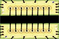
This bare die is well suited for integration into high density MCP (Multi-Chip-Package), MCM (Multi-Chip-Module) & SiP (System-In-Package) solutions. Supported by the highest quality KGD test flow, wafers deliver high reliability and superior yield.
Features:
- VDD = 1.8V ±0.1V, VDDQ = 1.8V ±0.1V
- JEDEC standard 1.8V I/O (SSTL_18-compatible)
- Double data rate interface: two data transfers per clock cycle
- Differential data strobe (DQS, DQS\)
- 4-bit prefetch architecture
- On chip DLL to align DQ and DQS transitions with CK
- 4 internal banks for concurrent operation
- Programmable CAS latency (CL) 3, 4, 5, and 6 supported
- Posted CAS and programmable additive latency (AL) 0, 1, 2, 3, 4, and 5 supported
- WRITE latency = READ latency - 1 tCK
- Programmable burst lengths: 4 or 8
- Adjustable data-output drive strength, full and reduced strength options
- On-die termination (ODT)
- Operation Temperature -40°C to 105°C
- Committed long term support with very low obsolescence or mask change rate.
Product Families: Used for this device are tabulated below.
Functional:
- Density: 512Mb
Specification:
Depth: 32M
Width: VS: 1.8V
Refresh: 8K
Speed: -MHz
Width: VS: 1.8V
Refresh: 8K
Speed: -MHz
Other Detail: Important information for this device is tabulated below.
Traffic light setting for Minimum Order Quantity indicates the following:
- Green:Available from stock or at low factory MOQ.
- Amber: Available on factory order with MOQ.
- Red: High factory MOQ may apply, please ask for details.
Traffic light setting for High Reliability indicates the following:
- Green: This bare die is specified and tested for use in high reliability applications.
- Amber: This bare die can meet higher reliability specifications with additional testing & qualification, please ask for details.
- Red: This bare die is not specified or specifically designed for use in high reliability applications.
Traffic light setting for Space Grade indicates the following:
- Green: This bare die is qualified for space applications or has space level qualification data, please ask for details.
- Amber: This bare die can be specified for space applications with additional testing and qualification, please ask for details.
- Red: Suitability of this bare die for space applications is unknown and requires further qualification, please ask for details.