- ** PRODUCT DISCONTINUED **
- Choice of two Phase Comparators:
- Exclusive Or Gate, duty cycle limited
- Rising edge switching, duty cycle unlimited.
- Buffered outputs compatible with MHTL and Low power TTL
- VCO inhibit control for ON-OFF keying and ultra-low standby power consumption
- Source-follower output of VCO control input
- Integrated zener diode to assist supply regulation
- High Input Voltage up to 20V
- Specified at 5V, 10V & 15V
- Military Temperature Range for High Reliability
- Smaller die size versus peers
SiS OBSOLETE
Electrical Datasheet
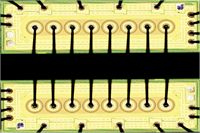
Die Physical Data:
Footprint: 4.265mm² (6611.235mil²)
Request Pad Layout
- Input Level: CMOS
- Output Level: CMOS
- Bits: 1
VCC (Max): 18.00V
fMIN @ VNOM: 8MHz
tpd (Max) @ VNOM: 300ns
ICC (Max) @ VNOM: 0.60mA
Output Drive (Max): 4.2mA
VNOM (Max): 15V
- Green:Available from stock or at low factory MOQ.
- Amber: Available on factory order with MOQ.
- Red: High factory MOQ may apply, please ask for details.
- Green: This bare die is specified and tested for use in high reliability applications.
- Amber: This bare die can meet higher reliability specifications with additional testing & qualification, please ask for details.
- Red: This bare die is not specified or specifically designed for use in high reliability applications.
- Green: This bare die is qualified for space applications or has space level qualification data, please ask for details.
- Amber: This bare die can be specified for space applications with additional testing and qualification, please ask for details.
- Red: Suitability of this bare die for space applications is unknown and requires further qualification, please ask for details.


