- Designed for 0.9V to 3.6V VCC Operation
- 2.9 ns tPD at 3.3V (Typ)
- Inputs/Outputs Over-Voltage Tolerant up to 3.6V
- IOFF Supports Partial Power Down Protection
- Source/Sink 2.6 mA at 3.3V
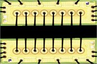
- Ultra-small bare die form factor.
ON Semi
Electrical Datasheet
Die Physical Data:
Footprint: 0.286mm² (442.681mil²)
Request Pad Layout
- Function: -
- Input Level: CMOS
- Output Level: CMOS
- Config: -
- 3-State O/P: No
VCC (Max): 3.60V
fMIN @ VNOM: 150MHz
tpd (Max) @ VNOM: 9.3ns
ICC (Max) @ VNOM: 0.001mA
VNOM (Max): 3.6V
- Bits: 1
- Function/Gate Type: -
- Input Level: CMOS
- Output Level: CMOS
VCC (Max): 3.60V
VNOM (Max): 3.60V
Output Drive (Max): 50mA
ICC (Max) @ VNOM: 0.0009mA
fMIN @ VNOM: 150MHz
tpd (Max) @ VNOM: 9.3ns
- Green:Available from stock or at low factory MOQ.
- Amber: Available on factory order with MOQ.
- Red: High factory MOQ may apply, please ask for details.
- Green: This bare die is specified and tested for use in high reliability applications.
- Amber: This bare die can meet higher reliability specifications with additional testing & qualification, please ask for details.
- Red: This bare die is not specified or specifically designed for use in high reliability applications.
- Green: This bare die is qualified for space applications or has space level qualification data, please ask for details.
- Amber: This bare die can be specified for space applications with additional testing and qualification, please ask for details.
- Red: Suitability of this bare die for space applications is unknown and requires further qualification, please ask for details.


