Operating with supply from 0.9V to 3.6V this bare die is optimised to combine high speed with low power and is well suited to applications with lower drive requirements. Form factor is also extremely small and suits size critical applications.
Features:
- 0.9V to 3.6V VCC supply operation
- 3.6V overvoltage tolerant I/Os at VCC from 0.9V to 3.6V
- tPD typ:
- 3.0 ns 3.0V - 3.6V VCC
- 4.0 ns 2.3V - 2.7V VCC
- 5.0 ns 1.65V - 1.95V VCC
- 7.0 ns 1.40V - 1.60V VCC
- 11.0 ns 1.10V - 1.30V VCC
- 30.0 ns 0.90V VCC
- Power-Off high impedance inputs and outputs
- Static Drive (IOH/IOL)
- ±2.6 mA @ 3.00V VCC
- ±2.1 mA @ 2.30V VCC
- ±1.5 mA @ 1.65V VCC
- ±1.0 mA @ 1.40V VCC
- ±0.5 mA @ 1.10V VCC
- ±20 µA @ 0.9V VCC
- Uses patented Quiet SeriesTM noise/EMI reduction circuitry
- Ultra-low dynamic power
- Ultra-small bare die form factor.
Vendor:
ON Semi
Electrical Datasheet
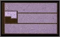
Die Physical Data:
Footprint: 0.286mm² (442.681mil²)
Request Pad Layout
ON Semi
Electrical Datasheet
Die Physical Data:
Footprint: 0.286mm² (442.681mil²)
Request Pad Layout
Product Families: Used for this device are tabulated below.
Functional:
- Bits: 1
- Function/Gate Type: -
- I/P Level: CMOS
- O/P Level: CMOS
Specification:
VCC (Min): 0.90V
VCC (Max): 3.60V
VNOM (Max): 3.60V
Output Drive (Max): 50mA
ICC (Max) @ VNOM: 0.0009mA
fMIN @ VNOM: 150MHz
tpd (Max) @ VNOM: 9.3ns
VCC (Max): 3.60V
VNOM (Max): 3.60V
Output Drive (Max): 50mA
ICC (Max) @ VNOM: 0.0009mA
fMIN @ VNOM: 150MHz
tpd (Max) @ VNOM: 9.3ns
Functional:
- Function: -
- I/P Level: CMOS
- O/P Level: CMOS
- Config: -
- 3-State O/P: No
Specification:
VCC (Min): 0.90V
VCC (Max): 3.60V
fMIN @ VNOM: 150MHz
tpd (Max) @ VNOM: 9.3ns
ICC (Max) @ VNOM: 0.001mA
VNOM (Max): 3.6V
VCC (Max): 3.60V
fMIN @ VNOM: 150MHz
tpd (Max) @ VNOM: 9.3ns
ICC (Max) @ VNOM: 0.001mA
VNOM (Max): 3.6V
Other Detail: Important information for this device is tabulated below.
Traffic light setting for Minimum Order Quantity indicates the following:
- Green:Available from stock or at low factory MOQ.
- Amber: Available on factory order with MOQ.
- Red: High factory MOQ may apply, please ask for details.
Traffic light setting for High Reliability indicates the following:
- Green: This bare die is specified and tested for use in high reliability applications.
- Amber: This bare die can meet higher reliability specifications with additional testing & qualification, please ask for details.
- Red: This bare die is not specified or specifically designed for use in high reliability applications.
Traffic light setting for Space Grade indicates the following:
- Green: This bare die is qualified for space applications or has space level qualification data, please ask for details.
- Amber: This bare die can be specified for space applications with additional testing and qualification, please ask for details.
- Red: Suitability of this bare die for space applications is unknown and requires further qualification, please ask for details.