- ** PRODUCT DISCONTINUED **
- Temperature compensated bandwidth (unity gain)
- Temperature compensated IB: 45nA
- Wide power supply range, single supply: 3V-32V or dual supplies: ±1.5V to ±16V
- Low VOS: 2mV, and IOS: 5nA
- Differential input voltage range equal to the power supply voltage
- Large output voltage: 0V to VCC -1.5V swing
- Input Common-Mode Voltage range includes ground
SiS OBSOLETE
Electrical Datasheet
Die Physical Data:
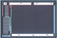
Footprint: 0.605mm² (937.443mil²)
Request Pad Layout
- Channels: 2
- Shutdown: No
VS (Max): 32.00V
Gain BW: 0.700MHz
Slew Rate: 0.30V/µs
VOS (Max): 7.000mV
VOS Drift: 7.000µV/°C
IIB (Max): 250.00000nA
VN: 40.0nV√Hz
IQ per Channel: 0.250mA
IO: 30.0mA
CMRR (Typ): 85dB
- Channels: 2
Gain BW: 0.700MHz
IIB (Max): 250.00000nA
VOS (Max): 7.000mV
IO: 30.0mA
IQ per Channel: 0.2500mA
Rail - Rail: Slew Rate: 0.30V/µs
VS (Max): 32.00V
VS (Min): 3.00V
VN: 40.0nV√Hz
VOS Drift: 7.0µV/°C
- Channels: 2
- Shutdown: No
Gain BW: 0.7000MHz
IIB (Max): 250,000.00pA
VOS (Max): 7.000mV
IO: 30.0mA
IQ per Channel: 0.25000mA
Rail - Rail: Slew Rate: 0.3000V/µs
VS (Max): 32.00V
VS (Min): 3.00V
VN: 40.0nV√Hz
VOS Drift: 7.000µV/°C
- Green:Available from stock or at low factory MOQ.
- Amber: Available on factory order with MOQ.
- Red: High factory MOQ may apply, please ask for details.
- Green: This bare die is specified and tested for use in high reliability applications.
- Amber: This bare die can meet higher reliability specifications with additional testing & qualification, please ask for details.
- Red: This bare die is not specified or specifically designed for use in high reliability applications.
- Green: This bare die is qualified for space applications or has space level qualification data, please ask for details.
- Amber: This bare die can be specified for space applications with additional testing and qualification, please ask for details.
- Red: Suitability of this bare die for space applications is unknown and requires further qualification, please ask for details.


