Background
SiP (System-In-Package) is not a new concept, packages described as SiPs have been designed, produced and in field use for quite some years. As an approach, it is general understood that a SiP bare die solution has multiple benefits providing a viable design can be realised and produced, the main advantage being high integration with size reduction. Generally SiP is defined as a package comprising multiple different dice which are interconnected to each other to form a modular system.
Influences on SiP design
Whilst the term SiP broadly infers a level of complex integration, the reality is that the complexity of SiP production changes relative to the bare die available, the interconnect technology versus target form factor and the design ecosystem. The final variable is the economic cost of production.
Availability of bare die
The commercial proposition of a SiP may suggest the potential for high sales volume down the road. Early hurdles to clear are establishing availability of bare die in low quantities for early prototypes and to produce a firm forecast to gain some idea of volume price-point + economic viability. There are many positives in using bare die and the main challenges are up-front around die product support from the vendor. This is because in many cases your needs may require a bare die maker to do something operationally unconventional or commercially outside of their comfort zone, see challenges of bare die for more details.
At diedevices.com we can assist by providing supported parts with known availability in bare die form.
Where a part is not supported we can either suggest available alternatives or act as the interface with the vendor to get bare die product released for which we have a successful track record and years of experience.
Interconnect technology versus target form factor
The desired outcome is the highest level of integration contained within the smallest package form factor. Bare die interconnect is a large contributor.
Below is a simplified example of industry interconnect types for SiP, there will be more complex multiple die variations on these themes:
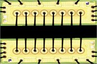
Wirebonding
The simplest wirebonded SiP assemblies are typically built as a stack in ascending order of die size with the SiP substrate providing the routing to circuit board. More complex variations of these stacks can be designed by the use of interposers which allow the bare die to be stacked in a configuration / order which best suits the electrical routing. The interposer also assists to increase the number of potential die in the stack. Wirebonding can also be used in mixed interconnect designs and in some cases is the only viable or effective way of adding extra die or enabling the SiP design e.g. MEMs integration.
Pro: Versatile, ease of availability, many existing bare die are mechanically compatible, can be integrated alongside other interconnect methods e.g. Flip-Chip
Con: Design rules mean X-Y-Z profile is larger, high I/O count devices push the limits of the technology in terms of die bond pad pitch & fan-out.
Wirebonding is a highly versatile way of connecting multiple dice to a substrate.
Flip-Chip
Flip-Chip assemblies utilize bare die material from three categories:
- Die originally mechanically produced for wirebond but made compatible via additional bump processing
- Die designed specifically for single package flip-chip
- Die designed specifically for 3D or vertical integration with TSV (Through Silicon Vias) or configurable RDL (Re-distribution layers)
Flip-Chip design / assembly focuses on higher density interconnect routing to the substrate and there are several methods of increasing complexity to achieve that.
Lower complexity flip-chip SiP focuses on routing via the SiP substrate, this typically Adding redistribution layers to the die original I/O layout, adding distribution layers by use of interposer(s) or routing through die-to-die by application specific interconnect or TSV are methods employed.
Pro: Most bare die can be modified for use as flip-chip, smaller form factor, shorter path lengths for performance and power
Con: Cost and complexity at lower volumes, additional cost of substrates, RDL and silicon interposer development. Highest integrations require mated die-to-die interconnect and complex design cycle.
The evolution of SiP bare die integration

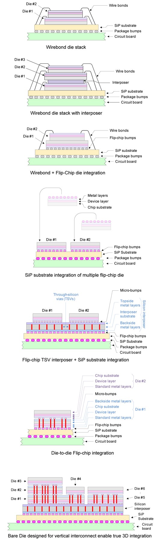
Above is a potential example of very high-end 3D integration.
SoC (System-On-Chip)
All features/technologies are full integrated monolithically within one die. The SiP becomes a single chip package with the challenge now focusing on routing i/o to the substrate.
However, this usually only applies for applications which can benefit from a very specific design contained within fab process capabilities and having the commercial business models to justify development expense. The cost of on-chip integration can also escalate drastically depending on the type and complexity of technologies that need to be combined. In many instances when technology types singly use very different fabrication processes the cost of creating a new fabrication process combining them is instantly prohibitive or may requires a production technology which isn't yet qualified or even in existence.
Looking forward
The use of bare die in SiP will continue to evolve as commercial markets are increasingly faced with a demand for further integration increase and size reduction. Emerging sectors such as IoT and sensor integration in general require a combination of technologies which to a large extent were formerly considered separate technology blocks, known in the industry as heterogeneous integration. Some of this can be achieved monolithically at wafer level however a large proportion will either be technology restricted or not make economic sense to do. This presents a bare die integration as a good contender solution to fill the gap. These knock-on effects may benefit users outside of the commercial sector by improving the seeding and numeracy of new complex high performance die products in respect of their target application. However there is also a risk that older mature technologies in the market see more effects of obsolescence as semiconductor consolidations through merger and acquisition change strategic product focuses.