Innovate > Integrate > Empower - Design at Die Level

Wafer and Die Level Testing

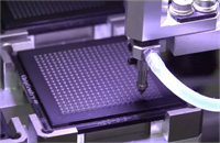
Below are the product familes, temperature options and data options that can be tested at the bare die level. Please note that custom test setups with additional parameters are also available on request.

Bare die Integrated Circuits

  • ADC - Up to 16-Bit Parallel / Serial
  • DAC - Up to 16-Bit Parallel / Serial
  • Multiplexers - 24 I/Os max
  • Operational Amplifiers & Comparators - Up to 10Mhz
  • Switches - 24 I/Os max
  • TTL, CMOS - 24 I/Os max
  • Voltage Regulators - All

Bare die Discrete Components

  • Diodes - Current Regulator, PiN, Rectifier, Schottky, Zener, TVS
  • Transistors - BJT, Darlington, JFET, MOSFET, IGBT, Thyristor / SCR, TRIAC  

Generic Test Coverage

  • Current Resolution: Picoamp 
  • Max Frequency – 20MHz
  • Max Voltage – 614V
  • Max Current – 50A (Pulsed) 4A (Continuous)
  • Test temperature - 25°C to 200°C
  • Full datalog or pass/fail
  • Optional grading / multiple binning.  
Standard parameter test capabilities by family:

Symbol Parameter Max test limit  Max reading 
V(BR)CEO, CES, CER Collector-Emitter Breakdown Voltage IC = 200mA 614V
V(BR)CBO Collector-Base Breakdown Voltage IC = 200mA 614V
V(BR)EBO Emitter-Base Breakdown Voltage IB = 50A 16V
VCE(sat) Collector-Emitter saturation voltage  IB = 50A  16V 
IC = 50A
 VBE(sat) Base-Emitter saturation voltage  IB = 50A  16V 
IC = 50A
VBE(on) Base-Emitter threshold voltage VCE = 10V 16V
IC = 50A
ICEO , ICES Collector cutoff current VCE = 614V 1mA
ICBO Collector cutoff current VCB = 614V 1mA
IEBO Emitter cutoff current VBE = 10V 100mA
VCE = 10V
hFE1  , hFE2 DC current gain factor VCE = 10V  2 x 10⁵
IC = 50A
IB = 50A 
h21e Short-circuit forward current ratio VCE = 10V  2 x 10⁵
IC = 1A
Symbol  Parameter  Max test limit  Max reading 
VOS, VIO Input offset voltage   VS = ± 51V  200mV 
IS(max) = 225mA 
VOUT(OS) = ±32V 
VRGOS Positive / negative supply current  VOUT = ± 30V  200mV 
IQ  Quiescent current  VS = ± 51V  250mA 
IS(max) = 225mA 
ΔVIN = 5V 
VOUT = 30V 
IB, IIB Input bias current  VS = ± 51V  20000nA 
IS(max) = 225mA 
VOUT(OS) = ± 30V 
IOS, IIO Input offset current  VS = ± 51V  20000nA 
IS(max) = 225mA 
VOUT(OS) = ± 30V 
AVO  Large-signal voltage gain  VS = ± 51V  130dB 
IS(max) = 225mA 
VOUT(OS) = ±32V 
IL = ± 255mA 
SR  Slew rate  VS = ± 15V  100V/μs 
VREF = ± 12V 
ΔVIN = ± 2V 
CMMR  Common-mode rejection ratio   VS = ± 51V  130dB 
IS(max) = 255mA 
ΔVIN = ± 51V 
PSSR  Power supply rejection ratio   VS = ± 51V  130dB 
IS(max) = 255mA 
ΔVS = ± 50V 
VO  Output voltage swing  VS = ± 51V  ± 51V 
IS(max) = 255mA 
IL = 255mA 
GBW Gain-bandwidth product  VS = ± 51V  200MHz 
Frequency range: 
10 to 100kHz 
ISC Output short-circuit current  VS = ± 51V  200mA 
VIN = ± 5V | VOUT = ± 16 V 
GM Forward transconductance  VS = ± 51V  7.5 x 10⁵mS 
Δ IS @ VS = ± 15V ~ 60 μA 
Symbol Parameter  Max test limit
VOL  Low-level output voltage  20V 
VOH High-level output voltage 20V
VIL Low-level input voltage 20V
VIH High-level input voltage 20V
IIL Low-level input current  10mA 
IIH High-level input current 10mA
IOL Low-level output current 10mA
IOH High-level output current  10mA 
IOZH, IOZL, IOZ High-impedance-state output current  10mA
ICCL , ICCH , ICC , IDD Quiescent current 200mA 
IOS Short-circuit output current   200mA 
VIK Input clamp voltage  10V 
VT Threshold voltage  20V 
RON On-state resistance  10kΩ 
  Continuity test  2V 
  Function test Pass / Fail
  Hysteresis  20V
Symbol  Parameter Max test limit  Max reading 
IR  Reverse current  VR = 614V  1mA 
V Reverse voltage  IR = 200mA  614V 
VF  Forward voltage  IF = 50A  10V 
VZ  Zener voltage  IZ = 50A  20V 
Symbol  Parameter  Max test limit  Max reading 
RDS (on)   Static drain-source on-state resistance  IDS = 50A  1kΩ 
VGS = 10V 
V(BR)DSS  Breakdown voltage drain-source  IDS = 200A  614V 
IDSS  Zero-gate-voltage drain current VDS = 614V  1mA 
VGS = 614V 
IGSSF   Forward gate current  VGS = 614V  1mA
IGSSR Reverse gate current VGS = 614V  1mA
VGS(th) Gate threshold voltage  IDS = 50A  10V 
VDS(on)  Drain source voltage  VGS = 10V  10V 
ID = 50A 
ID(on)  On-State Drain Current  VGS = 10V  50A 
VDS = 10V 
gfs  Forward Transconductance VDS = 10V  2000 S 
IDS = 50A 
Symbol  Parameter  Max test limit  Max reading 
VOS, VIO Input offset voltage   VS = ± 51V  200mV 
IS(max) = 225mA 
VOUT(OS) = ±32V 
VRGOS Positive / negative supply current  VOUT = ± 30V  200mV 
IQ  Quiescent current  VS = ± 51V  250mA 
IS(max) = 225mA 
ΔVIN = 5V 
VOUT = 30V 
IB, IIB Input bias current  VS = ± 51V  20000nA 
IS(max) = 225mA 
VOUT(OS) = ± 30V 
IOS, IIO Input offset current  VS = ± 51V  20000nA 
IS(max) = 225mA 
VOUT(OS) = ± 30V 
AVO  Large-signal voltage gain  VS = ± 51V  130dB 
IS(max) = 225mA 
VOUT(OS) = ±32V 
IL = ± 255mA 
SR  Slew rate  VS = ± 15V  100V/μs 
VREF = ± 12V 
ΔVIN = ± 2V 
CMMR  Common-mode rejection ratio   VS = ± 51V  130dB 
IS(max) = 255mA 
ΔVIN = ± 51V 
PSSR  Power supply rejection ratio   VS = ± 51V  130dB 
IS(max) = 255mA 
ΔVS = ± 50V 
VO  Output voltage swing  VS = ± 51V  ± 51V 
IS(max) = 255mA 
IL = 255mA 
GBW Gain-bandwidth product  VS = ± 51V  200MHz 
Frequency range: 
10 to 100kHz 
ISC Output short-circuit current  VS = ± 51V  200mA 
VIN = ± 5V | VOUT = ± 16 V 
GM Forward transconductance  VS = ± 51V  7.5 x 10⁵mS 
Δ IS @ VS = ± 15V ~ 60 μA 
Symbol Parameter Max test limit  Max reading 
V(BR)CEO, CES, CER Collector-Emitter Breakdown Voltage IC = 200mA 614V
V(BR)CBO Collector-Base Breakdown Voltage IC = 200mA 614V
V(BR)EBO Emitter-Base Breakdown Voltage IEB = 50A 10V
VCE(sat) Collector-Emitter saturation voltage  IB = 50A  10V 
IC = 50A
 VBE(sat) Base-Emitter saturation voltage  IB = 50A  10V 
IC = 50A
VBE(on) Base-Emitter threshold voltage IBE = 50A 10V
ICEO , ICBO, ICES,  ICER Collector cutoff current VCE = 20V 1mA
IEBO Emitter cutoff current VEB = 10V  100mA
hfe Small-signal DC current gain  VC = 10V  200V 
f = 1kHz 
Symbol Parameter Max test limit Max reading
VO Output voltage VIN = VO + 51V 5V
IL = 16A
RLINE Line regulation VIN1 = 56V 1500mV
VIN2 = 56V
IL = 16A
RLOAD Load regulation VIN = VO + 51V 1500mV
IL1 = 16A
IL2 = 16A
IQ Quiescent current VIN = VO + 51V 250mA
IL = 3.2 A
PSRR Power supply ripple rejection  VIN = VO + 51V 100dB 
IL = 295mA
Fmod = 2KHz
Vmod = 4Veff
ISC Short circuit current  VIN = VO + 51V 3.2A
VDROP Dropout voltage  VIN = VO + 51V 10V
IL = 16A
ΔVO = 1000mV
Vres Reset output voltage  VIN = VO + 51V 102V
IL = 255mA
ILEAK Reset leakage current  VIN = VO + 51V 200mA
IL = 255mA
VREV DC Reverse DC input voltage IR = 100mA 60V

H Screening Flow

Sample distribution - Single diffusion, Multiple Wafers

Sample size - 20 PCS (5 destruct)

Pre-Sample Assembly

Die Visual Inspection - MIL-STD-750/TM2072, MIL-STD-750/TM2071, MIL-STD-883/TM2010B

Sample Assembly

Die Attach - MIL-STD-883/TM2010

Die Shear Test - MIL-STD-883/TM2019

Die Attach Inspection - MIL-STD-883/TM2011

Wire bond – Internal spec 

Wire bond integrity - MIL-STD-883/TM2011

Pre-Cap inspection - MIL-STD-883/TM2010

Internal Die Visual - MIL-STD-883/TM2010B, MIL-STD-750/TM2072, MIL-STD-75/TM2073

Package seal - MIL-STD-883/TM1014

Seal Inspection - MIL-STD-883/TM2009

Sample coding – Internal spec

Sample Testing

Stability Bake - MIL-STD-883/TM1008

Interim Electrical Test @ 25°C - In accordance with device specification

Interim Electrical Test @ 125°C - In accordance with device specification

Interim Electrical Test @ -55°C - In accordance with device specification

120 hours burn-in @ 150°C - In accordance with device specification

Final Electrical Test @ 25°C - In accordance with device specification

Final Electrical Test @ 125°C - In accordance with device specification

Final Electrical Test @ -55°C - In accordance with device specification

Outgoing Die Release

From sample tested diffusion only

100% die visual inspection - MIL-STD-750/TM2072, MIL-STD-750/TM2071, MIL-STD-883/TM2010B

K Screening Flow

Sample distribution - Single diffusion, Single Wafer

Sample size - 20 PCS (5 destruct)

Pre-Sample Assembly

Die Visual Inspection - MIL-STD-750/TM2072, MIL-STD-750/TM2071, MIL-STD-883/TM2010B

SEM Inspection - Scanning Electron Microscopy – MIL-STD-883/TM2018

Sample Assembly

Die Attach - MIL-STD-883/TM2010

Die Shear Test  - MIL-STD-883/TM2019

Die Attach Inspection - MIL-STD-883/TM2010

Wire bond – Internal spec

Wire bond integrity - MIL-STD-883/TM2011

Pre-Cap inspection - MIL-STD-883/TM2010

Internal Die Visual - MIL-STD-883/TM2010A, MIL-STD-750/TM2072, MIL-STD-75/TM2073

Package seal - MIL-STD-883/TM1014

Seal Inspection - MIL-STD-883/TM2009

Sample coding – Internal spec

Sample Testing

Stability Bake - MIL-STD-883/TM1008

Temperature Cycle - MIL-STD-883/TM1010

Centrifuge - MIL-STD-883/TM2001

Interim Electrical Test @ 25°C - In accordance with device specification

Interim Electrical Test @ 125°C - In accordance with device specification

Interim Electrical Test @ -55°C - In accordance with device specification

120 hours burn-in @ 150°C - In accordance with device specification

Post 120-hour Electrical Test @ 25°C - In accordance with device specification

Post 120-hour Electrical Test @ 125°C - In accordance with device specification

Post 120-hour Electrical Test @ -55°C - In accordance with device specification

Steady State Life Test @ 150°C – MIL-STD-883/TM1005

Life burn-in 240 hours - MIL-STD-883/TM1015

Final Electrical Test @ 25°C - In accordance with device specification

Final Electrical Test @ 125°C - In accordance with device specification

Final Electrical Test @ -55°C - In accordance with device specification

Outgoing Die Release

From sample tested wafer only

100% die visual inspection - MIL-STD-883/TM2010A, MIL-STD-750/TM2072, MIL-STD-75/TM2073